Hello! Sign In or Register now
About Us Information Comment FeedBack APPBuy(0)
Inquiry(0)
Dear customers, due to the implementation of the GDPR policy in Europe, UTSOURCE has also made adjustment accordingly to meet the policy requirements. Please read the new privacy policy carefully and this window will no longer pop up after you accept it.
Delivery Address
+ Add Address
The new shipping address
* Please fill in the cell phone number correctly to make sure that you can receive the tracking info in time.
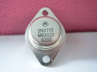
DESCRIPTION ● With TO-3 package ● Complement to type 2SB554 ● High power dissipation ● High collector-emitter breakdown voltage : VCEO=180V(min) APPLICATIONS ● Power amplifier applications
DESCRIPTION ●High Collector-Emitter Breakdown Voltage- V(BR)CEO= 230V(Min) ●Good Linearity of hFE●Complement to Type 2SA1295 APPLICATIONS ●Designed for audio and general purpose applications.
Off-Line SMPS Current Mode Controller with integrated 650V CoolMOSand Startup cell (frequency jitter Mode) in DIP-8 PG-DIP-8 Product Highlights●Active Burst Mode to reach the lowest Standby Power Requirements 100mW ●Adjustable Blanking Window for High Load Jumps to increase Reliability ●Frequency Jittering for Low EMI ●Pb-free lead plating, RoHS compilantFeatures ●650V Avalanche Rugged CoolMOSwith built in switchable Startup Cell●Active Burst Mode for lowest Standby Power @ light load controlled by Feedback Signal ●Fast Load Jump Response in Active Burst Mode ●67 kHz fixed Switching Frequency ●Auto Restart Mode for Over temperature Detection ●Auto Restart Mode for Overvoltage Detection ●Auto Restart Mode for Overload and Open Loop ●Auto Restart Mode for VCC Undervoltage ●User defined Soft Start ●Minimum of external Components required ●Max Duty Cycle 75% ●Overall Tolerance of Current Limiting ±5% ●Internal Leading Edge Blanking ●BiCMOS technology provides wide VCC Range ●Frequency Jittering for Low EMIDescription The CoolSET-F3(Jitter version) meets the requirements for Off-Line Battery Adapters and low cost SMPS for the lower power range. By use of a BiCMOS technology a wide VCC range up to 26V is provided. This covers the changes in the auxiliary supply voltage if a CV/CC regulation is implemented on the secondary side. Furthermore an Active Burst Mode is integrated to fullfill the lowest Standby Power Requirements 100mWat no load and Vin= 270VAC.As during Active Burst Mode the controller is always activethere is an immediate response on load jumps possiblewithout any black out in the SMPS. In Active Burst Modethe ripple of the output voltage can be reduced 1%. Furthermore Auto Restart Mode is entered in case of Overtemperature, VCC Overvoltage, Output Open loop or Overload and VCC Undervoltage. By means of the internal precise peak current limitation, the dimension of the transformer and the secondary diode can be lowered which leads to more cost efficiency.
Features●Timing From Microseconds to Hours●Astable or Monostable Operation●Adjustable Duty Cycle●TTL-Compatible Output Can Sink or SourceUp to 200 mA●On Products Compliant to MIL-PRF-38535,All Parameters Are Tested Unless OtherwiseNoted. On All Other Products, ProductionProcessing Does Not NecessarilyIncludeTesting of All Parameters.Applications●Fingerprint Biometrics●Iris Biometrics●RFID ReaderDescriptionThese devices are precision timing circuits capable ofproducing accurate time delays or oscillation. In thetime-delay or mono-stable mode of operation, thetimed interval is controlled by a single external resistor and capacitor network. In the a-stable modeof operation, the frequency and duty cycle can becontrolled independently with two external resistorsand a single external capacitor.The threshold and trigger levels normally are twothirds and one-third, respectively, ofVCCTheselevels can be altered by use of the control-voltageterminal. When the trigger input falls below the triggerlevel, the flip-flop is set, and the output goes high. Ifthe trigger input is above the trigger level and thethreshold input is above the threshold level, the flipflop is reset and the output is low. The reset (RESET)input can override all other inputs and can be used toinitiate a new timing cycle. When RESET goes low, the flip-flop is reset, and the output goes low. When the output is low, a low-impedance path is provided between discharge (DISCH) and ground.The output circuit is capable of sinking or sourcing current up to 200 mA. Operation is specified for supplies of 5 V to 15 V. With a 5-V supply, output levels are compatible with TTL inputs.
GENERAL DESCRIPTION The TDA1514A integrated circuit is a hi-fi power amplifier for use as a building block in radio, tv and other audio applications. The high performance of the IC meets the requirements of digital sources (e.g. Compact Disc equipment). The circuit is totally protected, the two output transistors both having thermal and SOAR protection.The circuit also has a mute function that can be arranged for a period after power-on with a delay time fixed by external components. The device is intended for symmetrical power supplies but an asymmetrical supply may also be used.Features ● High output power ● Low harmonic distortion ● Low intermodulation distortion ● Low offset voltage ● Good ripple rejection ● Mute/stand-by facilities ● Thermal protection ● Protected against electrostatic discharge ● No switch-on or switch-off clicks ● Very low thermal resistance ● Safe Operating Area (SOAR) protection
Descriptions ●General purpose amplifier ●High voltage application Features ●High collector breakdown voltage : VCBO= 180V, VCEO= 160V ●Low collector saturation voltage : VCE(sat)=0.5V(MAX.) ●Complementary pair with 2N5401
Features ●Capable of being mounted easily because of onepoint fixing type plastic molded package (Interchangeable with TO-3). ●Wide ASO because of on-chip ballast resistance. ●Good depenedence of fTon current and excellent high frequency responce.The descriptions in parentheses are for the 2SB817 only : other descriptions than those in parentheses are common to the 2SB817 and 2SD1047.
●OPERATING SUPPLY VOLTAGE UP TO 46 V ●TOTAL DC CURRENT UP TO 4 A ●LOW SATURATION VOLTAGE ●OVERTEMPERATURE PROTECTION ●LOGICAL ”0” INPUT VOLTAGE UP TO 1.5 V (HIGH NOISE IMMUNITY)DESCRIPTION The L298 is an integrated monolithic circuit in a 15- lead Multiwatt and PowerSO20 packages. It is a high voltage, high current dual full-bridge driver designedto acceptstandardTTL logic levels anddrive inductive loads such as relays, solenoids, DC and steppingmotors. Two enableinputs are providedto enableor disablethe deviceindependentlyof theinput signals. The emitters of the lower transistors of each bridge are connected togetherand the correspondingexternalterminal can be used for the connectionofanexternalsensingresistor.Anadditional supplyinput is provided so that the logic works at a lower voltage.
General Description Maxim’s DG300-DG303 and DG300A-DG303A CMOS dual and quad analog switches combine low power operation with fast switching times and superior DC and AC switch characteristics. On-resistance is less than 50Ωand is essentially constant over the analog signal range. Device specifications are ideal for batterypowered circuitry. These switches are available in a variety of formats as outlined in the Pin Configurations section. The switch control logic inputs are fully TTL and CMOS compatible. Also featured are “break-before-make” switching and low charge injection. Maxim’s DG300-DG303 and DG300A-DG303A families are electrically compatible and pin compatible with the original manufacturer’s devices. All devices operate with power supplies ranging from ±5V to ±18V. Single-supply operation is implemented by connecting V-to GND.Applications ●Portable Instruments ●Low-Power Sample/Holds ●Power-Supply Switching ●Programmable Gain Ampliffiers ●SPDT and DPDT Functions ●Process Control and TelemetryFeatures ●Monolithic Low-Power CMOS ●Latchup Proof Construction ●Fully Compatible 2nd Source ●Low On-Resistance, 50Ω●Fast Switching Time ●V+to V-Analog Signal Range ●Single-Supply Capability
Features ● Low Leakage Current ● Low Junction Capacitance ● High Mechanical Strength● Marking : Green cathode band ● Lead Free Finish/RoHS Compliant (P Suffix designates RoHS Compliant. See ordering information)Maximum Ratings ● Operating Temperature: -65℃to +75℃● Storage Temperature: -65℃to +75℃
Description●High-Performance M68HC08 Architecture●Fully Upward-Compatible Object Code with M6805, M146805, and M68HC05 Families●8.4 MHz Internal Bus Frequency●60 Kbytes of FLASH Electrically Erasable Read-Only Memory (FLASH) ●FLASH Data Security●1 Kbyte of On-Chip Electrically Erasable Programmable Read-Only Memory with Security Option(EEPROM)●2 Kbyte of On-Chip RAM●Clock Generator Module (CGM)●Serial Peripheral Interface Module (SPI)●Serial Communications Interface Module (SCI)Features●System Protection Features●Computer Operating Properly (COP) with Optional Reset
Features●Operating supply voltage 5 V to 28 V ●Typical RDSon = 150 mΩfor each output transistor (at 25℃) ●Continuous DC load current 5 A (TC 100℃) ●Output current limitation at typ. 6.6 A ±1.1 A ●Short circuit shut-down for output currents over 8 A ●Logic- inputs TTL/CMOS-compatible ●Output switching frequency up to 30 kHz ●Rise and fall times optimized for 0.5-2 kHz ●Over-temperature protection ●Short circuit protection ●Undervoltage disable function ●Diagnostic by SPI or Status-Flag (configurable) ●Enable and Disable inputs ●PG-DSO-20-37 power package ●Green Product (RoHS compliant)Functional Description The TLE 7209-2R is an intelligent full H-Bridge, designed for the control of DC and stepper motors in safety critical applications and under extreme environmental conditions. The H-Bridge is protected against over-temperature and short circuits and has an under voltage lockout for all the supply voltages “VS” (main DC power supply). All malfunctions cause the output stages to go tristate. The device is configurable by the DMS pin. When grounded, the device gives diagnostic information via a simple error flag. When supplied with VCC= 5 V, the device works in SPI mode. In this mode, detailed failure diagnosis is available via the serial interface.
DescriptionGOLD METALLISEDMULTI-PURPOSE SILICONDMOS RF FET10W -28V -1GHzSINGLE ENDED. PD Power DissipationBVDSS Drain -Source Breakdown VoltageBVGSS Gate -Source Breakdown Voltage ID(sat) Drain Current Tstg StorageTemperature Tj Maximum Operating Junction Temperature 70W 65V ±20V 8A-65 to 150℃200℃Features●SIMPLIFIED AMPLIFIER DESIGN●SUITABLE FOR BROAD BAND APPLICATIONS●LOW Crss●LOW NOISE●HIGH GAIN
Description: Powerex Application Specific IPMs (ASIPMs) are inteligent power modules that integrate power devices, gate drive and protection circuitry in a compact package for use in small inverter applications up to 20kHz. Use of application specific HVICs allow the designer to reduce inverter size and overall design time. Features: ● Compact Packages ● 3Phase Converter Bridge Built-in ● Integrated HVICs ● Direct Connection to DSP/CPU Applications: ● Small Motor Control ● Small Servo Motors ● General Purpose Inverters ● Pump and HVAC Motor Control
FEATURES ● Low Insertion Loss ● No Offset or Error Generated By Closed Switch - Purely Resistive - High Isolation Resistance From Driver ● Short Sample and Hold Aperture Time ● Fast Switching APPLICATIONS ● Analog Switches ● Choppers ● CommutatorsABSOLUTE MAXIMUM RATINGS (TA = 25℃unless otherwise specified) Gate-Drain or Gate-Source Voltage . . . . . . . . .... . . . . . . . 30V Gate Current . . . . . . . . . . . . . . . . . . . . .......... . . . . . 50mA Storage Temperature Range . . . . . . . . . .. . . . . -55℃to +150℃Operating Temperature Range . . . . . . . . . ... .. -55℃to +135℃Lead Temperature (Soldering, 10sec) . . . . . . . . . . .. . .. . 300℃Power Dissipation . . . . . . . . . . . . . . . . . . . . . . ....... . 350mW Derate above 25℃. . . . . . . . . . . . . . . . . . . . ... .. . 3.3mW/℃NOTE: Stresses above those listed under Absolute Maximum Ratings may cause permanent damage to the device. These are stress ratings only and functional operation of the device at these or any other conditions above those indicated in the operational sections of the specifications is not implied. Exposure to absolute maximum rating conditions for extended periods may affect device reliability.
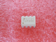
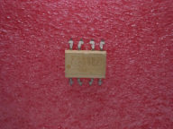
DescriptionThe PC123 is a miniature 1-Form-A solid state relay in a 4 pin SOP package that employs optically coupled MOSFETtechnology to provide 1500V of input to output isolation and is BSI certified for supplemental insulation in accordancewith EN60950. The efficient MOSFET switches and photovoltaic die use Clare’s patented OptoMOS architecture. Theoptically coupled input is controlled by a highly efficient GaAIAs infrared LED. The PC123 uses Clare’s state of the artdouble molded vertical construction packaging to produce the world’s smallest 4 pin relay. The PC123 offers board spacesavings of at least 20% over the competitor’s larger 4 pin SOP relay.Features●Small 4 Pin SOP Package●Low Drive Power Requirements (TTL/CMOS Compatible)●No Moving Parts●High Reliability●Arc-Free With No Snubbing Circuits●Supplemental Isolation●FCC Compatible●1500VRMS Input/Output Isolation●0.4mm Distance Through Insulation●FCC Compatible●No EMI/RFI Generation●Machine Insertable, Wave Solderable●Tape Reel Version Available
DESCRIPTION●Collector-Emitter Voltage-:VCER= 75V(Min);RBE=150Ω ●Collector Current- :IC=3A APPLICATIONS ●27MHz RF Power Amplifier Applications
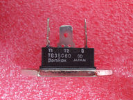
DescriptionThe ULN2002A, ULN2003A and ULN2004A are high voltage, high current Darlington arrays each containing seven open collector common emitter pairs. Each pair is rated at 500mA. Suppression diodes are included for inductive load driving, the inputs and outputs are pinned in opposition to simplify board layout. Device options are designed to be compatible with common logic families: ULN2002A (14-25V PMOS)ULN2003A (5V TTL, CMOS)ULN2004A (6-15V CMOS, PMOS)These devices are capable of driving a wide range of loads including solenoids, relays, DC motors, LED displays, filament lamps, thermal print-heads and high-power buffers. The ULN2002A, ULN2003A and ULN2004A are available in both a small outline 16-pin package (SO-16) and PDIP-16 package.Features:●500mA Rated Collector Current (Single Output)●High Voltage Outputs: 50V●Output Clamp Diodes●Inputs Compatible with Popular Logic Types●Relay Driver Applications●“Green”Molding Compound (No Br, Sb)●Totally Lead-Free Fully RoHS Compliant●Halogen and Antimony Free. “Green” Device
DescriptionThe 7805 5V fixed 3-terminal positive voltage regulator delivers up to 1.5A of output current with adequate heat-sinking. The device is equipped with internal limiting, safe-area compensation + thermal shutdown features for overload immunity. The 7805 can be used with external components to obtain adjustable voltages or currents can also be used as the power-pass element in precision high-current voltage regulators. No external components are needed other than to enhance performance or increase design flexibility.Features:●±5% VOUT tolerance over entire temperature range●Greater than 1A output current capability ●Internal thermal overload protection●Internal short-circuit current limit ●Output capacitor not essential for stability ●Full Military temperature range●Negative voltage complement is 7905
ApplicationsSTK4101II:6W min AF power amp.STK4111II: 10W min AF poweramp.STK4121II: 15W min AF poweramp.STK4131II: 20W min AF power amp.STK4141II: 25W min AF power amp.STK4151II: 30W min AFpower amp.STK4161II: 35W min AF power amp.STK4171II: 40W min AF power amp.STK4181II: 45W min AF power amp.STK4191II: 50W min AF power amp.FeatureBuilt-in muting transistor
DescriptionThe 74HC14 provides provides six independent Schmitt trigger input inverters with standard push-pull outputs. The device is designed for operation with a power supply range of 2.0V to 6.0V. The gates perform the Boolean function: Y = AFeatures●Wide Supply Voltage Range from 2.0V to 6.0V ●Sinks or Sources 4mA at VCC = 4.5V ●CMOS Low Power Consumption ●Schmitt Trigger Action at All Inputs ●ESD Protection Exceeds JESD 22200-V Machine Model (A115-A)2000-V Human Body Model (A114-A)Exceeds 1000-V Charged Device Model (C101C) ●Range of Package Options SO-14 and TSSOP-14 ●Totally Lead-Free Fully RoHS Compliant (Notes 1 2) ●Halogen and Antimony Free. “Green” Device (Note 3)Applications●General Purpose Logic ●Wide array of products such as:PCs, Networking, Notebooks, Netbooks Computer Peripherals, Hard Drives, CD/DVD ROMTV, DVD, DVR, Set Top Box
DescriptionThe VIPer12A combines a dedicated current mode PWM controller with a high voltage Power MOSFET on the samesilicon chip. Typical applications cover off line power supplies for battery charger adapters, standby power suppliesfor TV or monitors, auxiliary supplies for motor control, etc.Features●FIXED 60 KHZ SWITCHING FREQUENCY●9V TO 38V WIDE RANGE V DD VOLTAGE●CURRENT MODE CONTROL●AUXILIARY UNDERVOLTAGE LOCKOUTWITH HYSTERESIS●HIGH VOLTAGE START UP CURRENTSOURCE●OVERTEMPERATURE, OVERCURRENT ANDOVERVOLTAGE PROTECTION WITHAUTORESTART
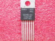
LM3886 OvertureTMAudio Power Amplifier Series High-Performance 68W Audio Power Amplifier w/MuteFeatures●68W Cont. Avg. Output Power into 4Ωat VCC=±28V●38W Cont. Avg. Output Power into 8Ωat VCC=±28V●50W Cont. Avg. Output Power into 8Ωat VCC=±35V●135W Instantaneous Peak Output PowerCapability●Signal-to-Noise Ratio≥92dB●An Input Mute Function●Output Protection from a Short to Ground orto the Supplies via Internal Current LimitingCircuitry●Output Over-Voltage Protection againstTransients from Inductive Loads●Supply Under-Voltage Protection, not AllowingInternal Biasing to Occur when |VEE| + |VCC|≤12V, thus Eliminating Turn-On and Turn-OffTransients●11-Lead TO-220 Package●Wide Supply Range 20V-94VAPPLICATIONS●Component stereo●Compact stereo●Self-powered speakers●Surround-sound amplifiers●High-end stereo TVsDESCRIPTIONThe LM3886 is a high-performance audio power amplifier capable of delivering 68W of continuous average power to a 40 load and 38W into 80 with 0.1% THD+N from 20Hz-20kHz.The performance of the LM3886, utilizing its Self Peak Instantaneous Temperature (°Ke) (Spike)protection circuitry, puts it in a class above discrete and hybrid amplifiers by providing an inherently dynamically protected Safe Operating Area (SOA). Spike protection means that these parts are completely safeguarded at the output against overvoltage, undervoltage, overloads, including shorts to the supplies, thermal runaway, and instantaneous temperature peaks.The LM3886 maintains an excellent signal-to-noise ratio of greater than 92dB with a typical low noise floor of 2.0μV. It exhibits extremely low THD+N values of 0.03% at the rated output into the rated load over the audio spectrum, and provides excellent linearity with an IMD (SMPTE)typical rating of 0.004%
Features1.High radiation resin mold package2.RMS ON-state current IT: 8 Arms at TC= 80℃(With heat sink ) 3.Built-in zero-cross circuit (S102S02/S202S02 ) 4.High repetitive peak OFF-state voltage S102S01/S102S02 VDRM : MIN. 400V S202S01/S202S02 VDRM : MIN. 600V 5.Isolation voltage between input and output( Viso: 4 000V rms)6.Approved by CSA, No. LR63705Recognized by UL, file No. E94758Applications1.Automatic vending machines, programmable controllers 2.Amusement equipment
The TA8435H is PWM chopper type sinusoidal micro stepbipolar stepping motor driver.Sinusoidal micro step operation is accomplished only aclock signal inputting by means of built-in hard ware.FEATURES●1 chip bipolar sinusoidal micro step stepping motordriver●Output current up to 1.5 A ( AVE ) and 2.5A ( PEAK )●PWM chopper type.●Structured by high voltage Bi-CMOS process technology.●Forward and reverse rotation are available.●2 , 1-2 , W1-2 , 2W1-2 phase 1 or 2 clock drives are selectable.●Package : HZIP25-P●Input Pull-up Resistor equipped with RESET Terminal R = 100 kΩ( Typ .)●Output Monitor available with Mo.lo ( Mo ) = ±2 MA ( MAX.)●Reset and Enable are available with RESET and ENABLE.
Low Noise Audio Amplifier Applications ●Recommended for first stages of EQ and M.C. head amplifiers. ●High |Yfs|: |Yfs| = 22 mS (typ.) (VDS= 10 V, VGS= 0, IDSS= 3 mA) ●High breakdown voltage: VGDS= -40 V ●Low noise: En = 0.95 nV/Hz1/2(typ.) (VDS = 10 V, ID = 1 mA, f = 1 kHz) ●High input impedance: IGSS= -1 nA (max) (VGS= -30 V)
DescriptionThe30521 is ideally suited for general purpose stepper motor applications in the automotive, industrial, medical and marineenvironment. The AMIS-30521 is intended for use in industrial applications. The 30521 version is qualified for use inautomotiveapplications.Features●On-Chip Current Translator●SPI Interface●Speed and Load-Angle Output●7 Step Modes from Full Step-up to 32 Micro-Steps●Fully Integrated Current-Sense●PWM Current Control with Automatic Selection of Fast and SlowDecay●Low EMC PWM with Selectable Voltage Slopes●Active Flyback Diodes●Full Output Protection and Diagnosis●Thermal Warning and Shutdown●Digital IO’s Compatible with 5 V and 3.3 V Microcontrollers●NCV Prefix for Automotive and Other Applications Requiring Siteand Control Changes
●VERY HIGH OPERATING VOLTAGE RANGE (±50V)●DMOS POWER STAGE●HIGH OUTPUT POWER (100W @ THD = 10%, RL= 8Ω, VS= ±40V)●MUTING/STAND-BY FUNCTIONS ●NO SWITCH ON/OFF NOISE ●VERY LOW DISTORTION ●VERY LOW NOISE ●SHORT CIRCUIT PROTECTED (WITH NO INPUT SIGNAL APPLIED) ●THERMAL SHUTDOWN ●CLIP DETECTOR ●MODULARITY (MORE DEVICES CAN BE EASILY CONNECTED IN PARALLEL TO DRIVE VERY LOW IMPEDANCES)DESCRIPTION TheTDA7293 is a monolithic integrated circuit in Multiwatt15 package, intended for use as audio class AB amplifier in Hi-Fi field applications (Home Stereo, self powered loudspeakers, Top-class TV). Thanks to the wide voltage range and to the high out current capability it is able to supply the highest power into both 4Ωand 8Ωloads. The built in muting function with turn on delay simplifies the remote operation avoiding switching on-off noises. Parallel mode is made possible by connecting more device through of pin11. High output power can be delivered to very low impedance loads, so optimizing the thermal dissipation of the system.
Features●Low Total Harmonic Distortion (THD)●Precise Adjustable Output Over-Voltage Protection●Open-Feedback Protection and Disable Function●Zero Current Detector●150μs Internal Start-up Timer●MOSFET Over-Current Protection●Under-Voltage Lockout with 3.5V Hysteresis●Low Start-up (40μA) and Operating Current (1.5mA)●Totem Pole Output with High State Clamp●+500/-800mA Peak Gate Drive Current●8-Pin DIP or 8-Pin SOP Applications●Adapter●Ballast●LCD TV, CRT TV●SMPSDescription The FAN7530 is an active power factor correction (PFC) controller for boost PFC applications that operates in critical conduction mode (CRM). It uses the voltage mode PWM that compares an internal ramp signal with the error amplifier output to generate MOSFET turn-off signal. Since the voltage mode CRM PFC controller does not need rectified AC line voltage information, it saves the power loss of the input voltage sensing network necessary for the current mode CRM PFC controller. FAN7530 provides many protection functions, such as over voltage protection, open-feedback protection, over-current protection, and under-voltage lockout protection. The FAN7530 can be disabled if the INV pin voltage is lower than 0.45V and the operating current decreases to 65μA. Using a new variable on-time control method, THD is lower than the conventional CRM boost PFC ICs.
1.5 A Adjustable Output, Positive Voltage Regulator The LM317 is an adjustable 3-terminal positive voltage regulator capable of supplying in excess of 1.5 A over an output voltage range of 1.2 V to 37 V. This voltage regulator is exceptionally easy to use and requires only two external resistors to set the output voltage. Further, it employs internal current limiting, thermal shutdown and safe area compensation, making it essentially blow-out proof. The LM317 serves a wide variety of applications including local, on card regulation. This device can also be used to make a programmable output regulator, or by connecting a fixed resistor between the adjustment and output, the LM317 can be used as a precision current regulator. ●Output Current in Excess of 1.5 A ●Output Adjustable between 1.2 V and 37 V ●Internal Thermal Overload Protection ●Internal Short Circuit Current Limiting Constant with Temperature ●Output Transistor Safe-Area Compensation ●Floating Operation for High Voltage Applications ●Available in Surface Mount D2PAK, and Standard 3-Lead Transistor Package ●Eliminates Stocking many Fixed Voltages