Lieferanschrift

Guten Tag! anmelden oder jetzt registrieren
APP Datenblatt Liveübertragung 290K likes Utsource

IC-Chips
Digitale integrierte Schaltkreise der Serie 74
Digitale integrierte Schaltungen der Serie CD40
Optische Koppler
Uhren- und Rechner-ICs
Operationelle Verstärker
Netzschalter Ics
Treiber Ics
Flash-Speicher
Speicher
Audio-Sonderzweck
Uhr/Timing - Anwendungsspezifisch
Uhr/Timing - Uhrenpuffer, Treiber
Takt/Timing - Taktgeneratoren, PLLs, Frequenzsynthesizer
Uhr/Timing - Verzögerungsleitungen
Uhr/Timing - IC-Batterien
Uhr/Timing - Programmierbare Zeitgeber und Oszillatoren
Uhr/Uhrzeit - Echtzeituhren
Datenerfassung - ADCs/DACs - Spezieller Zweck
Datenerfassung - Analoges Front-End (AFE)
Datenerfassung - Analog-Digital-Wandler (ADC)
Datenerfassung - Digitale Potentiometer
Datenerfassung - Digital-Analog-Wandler (DAC)
Datenerfassung - Touchscreen-Steuerungen
Eingebettet - CPLDs (Komplexe programmierbare Logikbausteine)
Eingebettet - DSP (Digitale Signalprozessoren)
Eingebettet - FPGAs (Field Programmable Gate Array)
Eingebettet - FPGAs (Field Programmable Gate Array) mit Mikrocontrollern
Eingebettet - Mikrocontroller, Mikroprozessor, FPGA-Module
Eingebettet - Mikrocontroller
Eingebettet - Mikrocontroller - Anwendungsspezifisch
Eingebettet - Mikroprozessoren
Eingebettete - PLDs (Programmable Logic Device)
Eingebettet - System On Chip (SoC)
Schnittstelle - Analogschalter - Spezialzweck
Schnittstelle - Analogschalter, Multiplexer, Demultiplexer
Schnittstelle - CODECs
Schnittstelle - Controller
Schnittstelle - Direkte digitale Synthese (DDS)
Schnittstelle - Treiber, Empfänger, Transceiver
Schnittstelle - Encoder, Decoder, Konverter
Schnittstelle - Filter - Aktiv
Schnittstelle - E/A-Expander
Schnittstelle - Modems - ICs und Module
Schnittstelle - Module
Schnittstelle - Sensor- und Detektor-Schnittstellen
Schnittstelle - Sensor, kapazitive Berührung
Schnittstelle - Serialisierer, Deserialisierer
Schnittstelle - Signalpuffer, Repeater, Splitter
Schnittstelle - Signalabschlusswiderstände
Schnittstelle - Spezialisiert
Schnittstelle - Telekommunikation
Schnittstelle - UARTs (Universal Asynchronous Receiver Transmitter)
Schnittstelle - Sprachaufzeichnung und -wiedergabe
Linear - Verstärker - Audio
Linear - Verstärker - Instrumentierung, OP-Verstärker, Pufferverstärker
Linear - Verstärker - Spezialzweck
Linear - Verstärker - Videoverstärker und -module
Lineare - Analoge Multiplikatoren, Dividierer
Linear - Komparatoren
Linear - Videoverarbeitung
Logik - Puffer, Treiber, Empfänger, Transceiver
Logik - Komparatoren
Logik - Zähler, Dividierer
Logik - FIFO-Speicher
Logik - Flip-Flops
Logik - Tore und Umkehrer
Logik - Tore und Wechselrichter - Multifunktion, konfigurierbar
Logik - Verriegelungen
Logik - Multivibratoren
Logik - Paritätsgeneratoren und Prüfer
Logik - Schieberegister
Logik - Signalumschalter, Multiplexer, Decoder
Logik - Fachgebietslogik
Logik - Übersetzer, Level-Shifter
Logik - Universalbus-Funktionen
Speicher - Batterien
Speicher - Konfigurationsprogramme für FPGAs
Speicher - Controller
PMIC - AC-DC-Wandler, Offline-Schalter
PMIC - Batterieladegeräte
PMIC - Batterie-Management
PMIC - Aktuelle Regulierung/Verwaltung
PMIC - Anzeige-Treiber
PMIC - Energiemessung
PMIC - Volle, halbe Brückentreiber
PMIC - Gate-Treiber
PMIC - Hot-Swap-Steuerungen
PMIC - Laser-Treiber
PMIC - LED-Treiber
PMIC - Beleuchtung, Vorschaltgerätesteuerungen
PMIC - Motortreiber, Steuerungen
PMIC - OR-Steuerungen, ideale Dioden
PMIC - PFC (Leistungsfaktor-Korrektur)
PMIC - Stromverteilungsschalter, Lasttreiber
PMIC - Energieverwaltung - Spezialisiert
PMIC - Power-over-Ethernet (PoE)-Steuerungen
PMIC - Stromversorgungs-Controller, Monitore
PMIC - RMS-DC-Wandler
PMIC - Aufsichtsbehörden
PMIC - Thermisches Management
PMIC - V/F- und F/V-Wandler
PMIC - Spannungs-Referenz
PMIC - Spannungsregler - DC-Schalt-Controller
PMIC - Spannungsregler - DC-Schaltregler - DC-Schaltregler
PMIC - Spannungsregler - Linear
PMIC - Spannungsregler - Linear + Schalten
PMIC - Spannungsregler - Lineare Regler Regler
PMIC - Spannungsregler - Spezieller Zweck
Spezialisierte ICs
Module
IGBT
IPM
Thyristoren
Gleichrichter
Die Stromversorgung
Intelligentes Leistungsmodul
SCR,GTO und Diode
FET
Darlington-Transistoren
RF-Module
CNC-PRODUKTE
ENCODER
Motor
Servoantrieb & Verstärker & Servo
Dioden-Modul
Transistor-Modul
Schalter-Relais
PLC
Wechselrichter
Schütz und Unterbrecher
Aufzug-Brett
Industrielle Steuerung
Bipolartransistoren
Diode
Bipolare Transistoren
Widerstände
Kohlefilmwiderstände
Zementwiderstände
Chassis Mount-Widerstände
Chassis Mount-Widerstände
Strommesswiderstände
Schmelzbarer Chip-Widerstand
Hochpräzise & Low TCR SMD Widerstände
Hochspannungswiderstand
LED-Streifenwiderstände
MELF-Widerstand
Metalllegierungswiderstände
Metallfilm-Widerstand (TH)
Metall-Lasur-Widerstände
Metalloxidschichtwiderstände
Metalloxidwiderstände
NTC-Thermistoren
PTC-Thermistoren
Photoresistoren
Potentiometer & variable Widerstände
Präzisions-Potentiometer
Widerstandsnetzwerke & -anordnungen
Widerstandsnetzwerke und -arrays (TH)
Ultra-Niederwiderstände (SMD)
Variable Widerstände
Varistoren
Drahtgewickelte Widerstände
Kondensatore
Aluminium-Elektrolyt-Kondensatoren - SMD
CL21 Kondensator
Keramische Scheibenkondensatoren
Hochspannungskondensatoren
Metallisierter Polyesterfolienkondensator
Mehrschichtige Keramikkondensatoren MLCC - Bedrahtet
Mehrschichtige Keramikkondensatoren MLCC - SMD/SMT
Mylar-Kondensator
Nioboxid-Kondensatoren
Polyester-Filmkondensatoren
Solid Polymer Elektrolytkondensator
Superkondensatoren & Ultrakondensatoren
Entstörkondensatoren
Tantalkondensatoren
Trimmer, variable Kondensatoren
Induktivitäten
Antennen
Stromwandler
Allgemeine Induktoren (TH)
HF-Induktoren
Induktoren (SMD)
Leitungsfilter
Leistungsinduktoren
Leistungstransformator
RJ45 Transformator
Radialer Induktor (TH)
Die kreisförmigen Induktoren
Quarze Oszillatoren
49S
49SMD
49U
Keramische Resonatoren
DIP-Oszillatoren (XO)
Radialzylinderkristalle
SAW-Resonatoren
SMD-Kristalle
SMD-Oszillatoren (XO)
Steckverbinder
AV-Anschlüsse
Audio- und Videoanschlüsse
Bananen- und Spitzenanschlüsse
Kartenrandverbinder
Rundsteckverbinder
Steckverbinder - Kartensteckplätze
Steckverbinder
Steckverbinder - Zubehör
Steckverbinder - Gehäuse
Kontakte
D-Sub-Steckverbinder
Ethernet-Steckverbinder/Modularsteckverbinder
FFC, FPC (Flat Flexible) Steckverbinder
Lichtwellenleiter-Steckverbinder
IC- und Komponentensockel
LED-Lichtleiter
Mezzanine-Steckverbinder (Board to Board)
Leiterplattensteckverbinder - Stiftleisten, Stecker und Pins
Leiterplattensteckverbinder - Stiftleisten, Buchsen, Buchsen, Buchsenleisten
Leiterplattensteckverbinder - Gehäuse
Leistungssteckverbinder
HF-Steckverbinder/Koaxialsteckverbinder
Shunts & Jumper
Reihenklemmen - Zubehör
Reihenklemmen - Barriereklemmen
Reihenklemmen - DIN-Schiene, Kanal
Anschlussklemmen - Stiftleisten, Stecker und Buchsen
Terminals
Testclips
Prüfpunkte/Testringe
USB-Anschlüsse
Nicht spezifizierte Steckverbinder
Schraubverdrahtung
Federverdrahtung
Steckbare Reihenklemmen
Durchwandklemmen
Kfz-Terminals
Klemmengehäuse, Isolierhülsen und -blöcke
Schnelltrenn-Kabelverbinder und -klemmen
Ersatz- und Verschleißwerkzeuge
Kfz-Steckverbinder
Leiterplattensteckverbinder
SFP-Transceiver
100BASE SFP
1000BASE SFP
CWDM SFP
DWDM SFP
BIDI SFP
SONET/SDH SFP
2G/4G FC SFP
Customized SFP
SFP+ Transceiver
10G SFP+
BiDi SFP+
CWDM SFP+
DWDM SFP+
8G/16G FC SFP+
Customized SFP+
XFP-Transceiver
10G XFP
BIDI XFP
CWDM XFP
DWDM XFP
Customized XFP
40G/100G Transceiver
40G QSFP+
100G QSFP28
100G CFP
100G CFP2
100G CFP4
Customized 40G/100G
25G SFP28
100G CXP
40G BiDi QSFP+
Aktives optisches Kabel
10G SFP+ to SFP+ AOC
40G QSFP+ to QSFP+ AOC
40G QSFP+ to 4xSFP+ AOC
40G QSFP+ to 8xLC AOC
100G QSFP28 AOC
Customized AOC
25G SFP28 AOC
100G QSFP28 to 4xSFP28 AOC
56G QSFP+ to QSFP+
Direkt angebundene Kabel
10G SFP+ to SFP+ DAC
40G QSFP+ to QSFP+ DAC
40G QSFP+ to 4xSFP+ DAC
25G SFP28 to SFP28 DAC
100G QSFP28 to QSFP28 DAC
100G QSFP28 to 4 SFP28 DAC
Customized DAC
56G QSFP+ to QSFP+
Glasfaser HDMI-Kabel
Lichtwellenleiter Patchkabel
MTP/MPO Plenum Trunks
MTP/MPO-LC Plenum
MTP/MPO LSZH Trunks
MTP/MPO-LC LSZH
OM4 40 100Gb 50/125 Multimode
OM3 10Gb 50/125 Multimode
OM2 50/125 Multimode
OM1 62.5/125 Multimode
OS2 9/125 Singlemode Simplex
OS2 9/125 Singlemode Duplex
OM5 40G 100G 50/125 Multimode
Switchable LC Cables
Uniboot LC Cables
Ultra Low Loss LC SMF
Ultra Low Loss LC MMF
BIF Fiber Cables
Armored Patch Cables
Weitere Transceiver
Converter Modules
3G/HD-SDI SFP
GBIC Transceivers
PON Transcievers
Transceiver Accessories
Temperatursensoren
Temperatur-Schalter
Temperatur- und Feuchtigkeitssensor
Staubsensor
PM2.5-Sensor
Gassensor
Sensor für brennbare Gase
Alkohol-Sensor
CO-Sensor
Wasserstoffsensor
H2S-Sensor
CO2-Sensor
Ammonia Sensor
Formaldehyd-Sensor
PIR-Sensor
Andere Sensoren
Herzfrequenzsensor
Optischer Sensor
Farbsensor
Ultraschallsensor
Magnetfeldsensor
Stromsensor
Spannungssensor
Füllstandsensor für Flüssigkeiten
Sensor für atmosphärischen Luftdruck
Wettersensor
Neigungswinkelsensor
Bewegungssensor
Berührungssensor
Feuersensor
Vibrationssensor
Geschwindigkeitssensor
LED-Module
Hochleistungs-LED
SMD-LED
LED-Hintergrundbeleuchtung
COB-LED
LED-Anzeige
Plug-in LED
Infrarot-Induktion
Piranha-LED
LED-Lampen
Lichtemittierende Diode
LED-Leuchtmittel Chips
LED Epitaxial Wafer
Rotlicht-LED
Orangelicht-LED
Gelblicht-LED
Grün-/Gelblicht-LED
Grünlicht-LED
Blaulicht-LED
Violettlicht-LED
Weißlicht-LED
Weitere LED-Leuchtmittel Chips
LED-Anzeige


 Required
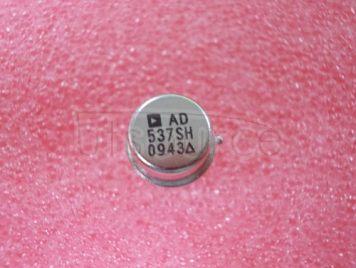
 frequency up to 100 kHz and any F.S. input voltage up to ±30 V. Linearity error is as low as ±0.05% for 10 kHz F.S., and operation is guaranteed over an 80 dB dynamic range. The overall temperature coefficient (excluding the effects of external components) is typically ±30 ppm/°C. The AD537 operates from a single supply of 5 V to 36 V and consumes only 1.2 mA quiescent current.
A temperature-proportional output, scaled to 1.00 mV/K, enables the circuit to be used as a reliable temperature-to-frequency converter<br/> in combination with the fixed reference output of 1.00 V, offset scales such as 0°C or 0°F can be generated.
The low drift (1μV/°C typ) input amplifier allows operation directly from small signals (e.g., thermocouples or strain gages) while offering a high (250 M(Ohm) input resistance. Unlike most V-F converters, the AD537 provides a square-wave output, and can drive up to 12 TTL loads, LEDs, very long cables, etc.
The excellent temperature characteristics and long-term stability of the AD537 are guaranteed by the primary bandgap reference generator and the low T.C. silicon chromium thin film resistors used throughout.
The device is available in either a TO-116 ceramic DIP or a TO-100 metal can<br/> both are hermetically sealed packages.
The AD537 is available in three performance/temperature grades<br/> the J and K grades are specified for operation over the 0°C to +70°C range while the AD537S is specified for operation over the extended temperature range, -55°C to +125°C.")