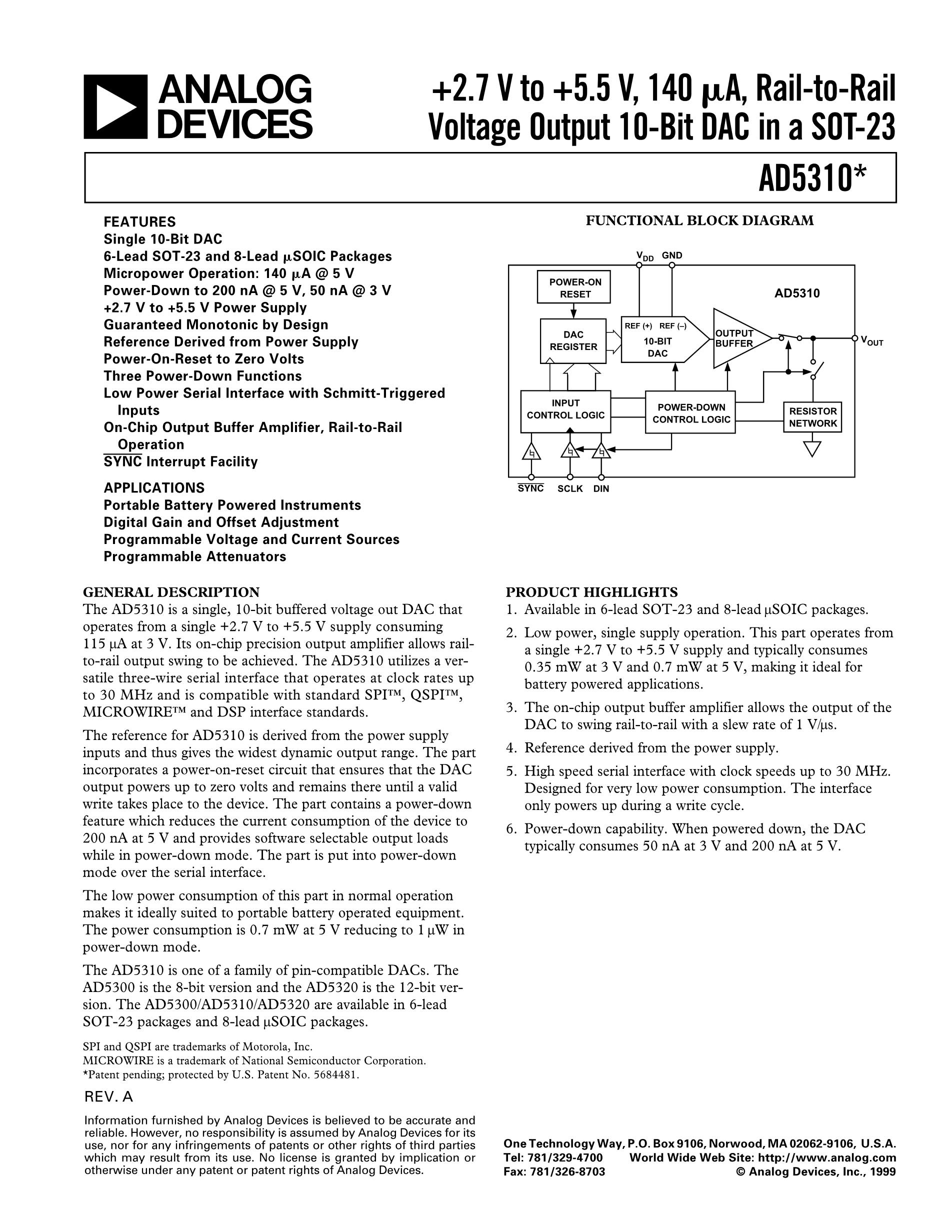
FEATURES
Pretrimmed (AD532K) No external components required Guaranteed ±1.0% maximum 4-quadrant error (AD532K) Differential inputs for Y2)/10 V transfer function Monolithic construction, low cost
APPLICATIONS
Multiplication, division, squaring, square rooting Algebraic computation Power measurements Instrumentation applications Available in chip form
The AD532 is the first pretrimmed, single chip, monolithic multiplier/divider. It guarantees a maximum multiplying error of ±1.0% and ±10 V output voltage without the need for any external trimming resistors or output op amp. Because the AD532 is internally trimmed, its simplicity of use provides design engineers with an attractive alternative to modular multipliers, and its monolithic construction provides significant advantages in size, reliability, and economy. Further, the AD532 can be a direct replacement for other IC multipliers that require external trim networks.
The AD532 multiplies in four quadrants with a transfer function Y2)/10 V, divides in two quadrants with - X2) transfer function, and square roots in one quadrant with a transfer function Z. In addition to these basic
functions, the differential X and Y inputs provide significant operating flexibility both for algebraic computation and transducer instrumentation applications. Transfer functions, such ±X2/10 V, and - X2), are easily attained and are extremely useful in many modulation and function generation applications, as well as in trigonometric calculations for airborne navigation and guidance applications, where the monolithic construction and small size of the AD532 offer considerable system advantages. In addition, the high commonmode rejection ratio (CMRR) (75 dB) of the differential inputs makes the AD532 especially well qualified for instrumentation applications, as it can provide an output signal that is the product of two transducer generated input signals.
The AD532J and AD532K are specified for maximum multiplying errors of ±2% and ±1% of full scale, respectively at 25°C, and are rated for operation from to 70°C. The AD532S has a maximum multiplying error ±1% of full scale it is also 100% tested to guarantee a maximum error ±4% at the extended operating temperature limits of -55°C and +125°C. All devices are available in either a hermetically sealed TO-100 metal can 14-lead D-14 side brazed ceramic DIP. The J, K, and S grade chips are also available.
1. True ratiometric trim for improved power supply rejection. 2. Reduced power requirements since no networks across
supplies are required. 3. More reliable because standard monolithic assembly
techniques can be used rather than more complex hybrid approaches. 4. High impedance X and Y inputs with negligible circuit loading. 5. Differential X and Y inputs for noise rejection and additional computational flexibility.
Information furnished by Analog Devices is believed to be accurate and reliable. However, no
responsibility is assumed by Analog Devices for its use, nor for any infringements of patents or other
rights of third parties that may result from its use. Specifications subject to change without notice. No
license is granted by implication or otherwise under any patent or patent rights of Analog Devices.
Trademarks and registered trademarks are the property of their respective owners.
Tel: 781.329.4700 ©20012015 Analog Devices, Inc. All rights reserved.
Features : 1 Applications : 1 General Description : 1 Flexibility of Operation : 1 Functional Block Diagram : 1 Guaranteed Performance Over Temperature : 1 Advantages of On The Chip Trimming of The Monolithic : 1 Revision History : 2 Specifications : 3 Thermal Resistance : 5
Chip Dimensions And Bonding Diagram : 5 ESD Caution : 5 Pin Configuration and Function Descriptions : 6 Typical Performance Characteristics : 7
D to Rev. E Deleted E-20-1 Package : Throughout Changes to Guaranteed Performance Over Temperature Section : 1 Deleted Figure 4; Renumbered Sequentially : 6 Deleted Table 4; Renumbered Sequentially : 7 Changes to Figure 14, Figure 15, and Figure : 11 Changes to Figure 17 and Figure : 12 Added Additional Information Section : 12 Updated Outline Dimensions : 13 Changes to Ordering Guide : 14
C to Rev. D Updated Format : Universal Added Pin Configuration and Function Descriptions Section : 6 Added Typical Performance Characteristics Section : 8 Changes to Figure : 8 Changes to Figure 12 and Figure : 9 Changes to Ordering Guide : 15
Nonlinearity 10 AC Feedthrough : 10 Common-Mode Rejection : 10 Dynamic Characteristics : 10 Power Supply Considerations : 10 Noise Characteristics : 10 Applications : 11 Replacing Other IC Multipliers : 11 Square Root : 12 Difference of Squares : 12 Additional Information : 12 Outline Dimensions : 13 Ordering Guide : 13
SPECIFICATIONS
Total Error TA = Minimum to Maximum Total Error vs. Temperature Supply Rejection Nonlinearity, X Nonlinearity, Y Feedthrough, X
DYNAMICS Small Signal BW 1% Amplitude Error Slew Rate Settling Time
OUTPUT Voltage Swing Impedance Offset Voltage Offset Voltage vs. Temperature Offset Voltage vs. Supply
X, Y Inputs X, Y Inputs TMIN to TMAX Z Input Z Input TMIN to TMAX Offset Current Differential Resistance DIVIDER PERFORMANCE Transfer Function Total Error


 Required
.")