ICチップ

74シリーズデジタル集積回路

CD40シリーズデジタル集積回路

光カプラー

クロック&電卓IC

オペアンプ

電源スイッチIcs

ドライバーIcs

フラッシュメモリー

記憶

オーディオの特別な目的

クロック/タイミング-アプリケーション固有

クロック/タイミング-クロックバッファー、ドライバー

クロック/タイミング-クロックジェネレータ、PLL、周波数シンセサイザ

クロック/タイミング-遅延線

クロック/タイミング-ICバッテリー

クロック/タイミング-プログラマブルタイマーおよび発振器

クロック/タイミング-リアルタイムクロック

データ集録-ADC / DAC-特別な目的

データ集録-アナログフロントエンド(AFE)

データ集録-アナログデジタルコンバーター(ADC)

データ収集-デジタルポテンショメータ

データ集録-デジタルアナログコンバーター(DAC)

データ収集-タッチスクリーンコントローラー

組み込み-CPLD(複雑なプログラマブルロジックデバイス)

組み込み-DSP(デジタルシグナルプロセッサ)

組み込み-FPGA(フィールドプログラマブルゲートアレイ)

組み込み-マイクロコントローラーを備えたFPGA(フィールドプログラマブルゲートアレイ)

組み込み-マイクロコントローラー、マイクロプロセッサー、FPGAモジュール

組み込み-マイクロコントローラー

組み込み-マイクロコントローラ-アプリケーション固有

組み込み-マイクロプロセッサ

組み込み-PLD(プログラマブルロジックデバイス)

組み込み-システムオンチップ(SoC)

インターフェイス-アナログスイッチ-特別な目的

インターフェイス-アナログスイッチ、マルチプレクサ、デマルチプレクサ

インターフェイス-コーデック

インターフェース-コントローラ

インターフェイス-ダイレクトデジタルシンセシス(DDS)

インターフェース-ドライバー、レシーバー、トランシーバー

インターフェース-エンコーダー、デコーダー、コンバーター

インターフェース-フィルター-アクティブ

インターフェイス-I / Oエクスパンダー

インターフェイス-モデム-ICおよびモジュール

インターフェース-モジュール

インターフェース-センサーと検出器のインターフェース

インターフェース-センサー、静電容量式タッチ

インターフェース-シリアライザ、デシリアライザ

インターフェース-信号バッファー、リピーター、スプリッター

インターフェース-シグナルターミネーター

インターフェース-特定品

インターフェース-テレコム

インターフェイス-UART(ユニバーサル非同期レシーバートランスミッター)

インターフェイス-音声の録音と再生

リニア-アンプ-オーディオ

リニア-アンプ-計装、OPアンプ、バッファアンプ

リニア-アンプ-特別な目的

リニア-アンプ-ビデオアンプおよびモジュール

線形-アナログ乗算器、除算器

線形-コンパレータ

リニア-ビデオ処理

ロジック-バッファー、ドライバー、レシーバー、トランシーバー

ロジック-コンパレータ

ロジック-カウンター、除算器

ロジック-FIFOメモリ

ロジック-フリップフロップ

ロジック-ゲートとインバータ

ロジック-ゲートおよびインバータ-多機能、構成可能

ロジック-ラッチ

ロジック-マルチバイブレーター

ロジック-パリティジェネレーターとチェッカー

ロジック-シフトレジスタ

ロジック-信号スイッチ、マルチプレクサ、デコーダ

ロジック-特殊ロジック

ロジック-トランスレータ、レベルシフタ

ロジック-ユニバーサルバス関数

メモリ-バッテリー

メモリ-FPGAの構成プロム

メモリ-コントローラ

PMIC-AC DCコンバーター、オフラインスイッチャー

PMIC-バッテリー充電器

PMIC-バッテリー管理

PMIC-現在の規制/管理

PMIC-ディスプレイドライバー

PMIC-エネルギー計測

PMIC-フル、ハーフブリッジドライバー

PMIC-ゲートドライバ

PMIC-ホットスワップコントローラ

PMIC-レーザードライバー

PMIC-LEDドライバ

PMIC-照明、バラストコントローラ

PMIC-モータードライバー、コントローラー

PMIC-ORコントローラ、理想ダイオード

PMIC-PFC(力率補正)

PMIC-配電スイッチ、負荷ドライバー

PMIC-電源管理-専門

PMIC-Power over Ethernet(PoE)コントローラ

PMIC-電源コントローラー、モニター

PMIC-RMSからDCへのコンバータ

PMIC-スーパーバイザ

PMIC-熱管理

PMIC-V / FおよびF / Vコンバーター

PMIC-電圧リファレンス

PMIC-電圧レギュレータ-DC DCスイッチングコントローラ

PMIC-電圧レギュレータ-DC DCスイッチングレギュレータ

PMIC-電圧レギュレータ-リニア

PMIC-電圧レギュレータ-リニア+スイッチング

PMIC-電圧レギュレータ-リニアレギュレータコントローラ

PMIC-電圧レギュレータ-特別な目的

専用IC

モジュール

IGBT

IPM

サイリスタ

整流器

電源

スマートパワーモジュール

SCR、GTOおよびダイオード

FET

ダーリントントランジスタ

RFモジュール

CNC製品

エンコーダー

モーター

サーボドライブ&アンプ&サーボ

ダイオードモジュール

トランジスタモジュール

スイッチリレー

PLC

インバーター

接触器とブレーカー

エレベーターボード

業界管理

トランジスタ

ダイオード

バイポーラトランジスタ

电阻

カーボンファイバー抵抗器

セメント抵抗器

シャーシマウント抵抗器

チップ抵抗器

電流検出抵抗器

可溶性チップ抵抗器

高精度&低抵抗温度計数 表面実装抵抗器

高電圧抵抗器

LEDストリップ抵抗器

MELE抵抗器

合金抵抗器

金属フィルム抵抗器(TH)

メタルグレーズ抵抗器

金属酸化フィルム抵抗器

金属酸化抵抗器

NTCサーミスタ

PTCサーミスタ

フォトレジスタ

ポテンショメータ&可変抵抗器

精密ポテンショメータ

抵抗器ネットワーク&配列

抵抗器ネットワーク&配列(TH)

超低抵抗器(SMD)

可変抵抗器

バリスタ

巻線抵抗器

电容

アルミニウム電解コンデンサーーSMD

CL21コンデンサー

セラミックディスクコンデンサー

高電圧コンデンサー

メタライズポリエステルフィルムコンデンサー

多層セラミックコンデンサーMLCC-有鉛

多層セラミックコンデンサーMLCC-SMD/SMT

マイラーコンデンサー

ニオブオキシドコンデンサー

ポリエステルフィルムコンデンサー

固体ポリマー電解コンデンサー

スーパーコンデンサー&ウルトラコンデンサー

抑制コンデンサー

タンタルコンデンサー

トリマー、可変式コンデンサー

インダクター&

アンテナ

電流トランスフォーマー

一般インダクター(TH)

HFインダクター

インダクター(SMD)

LINEフィルター

パワーインダクター

パワートランスフォーマー

RJ45トランスフォーマー

ラディカル・インダクター(TH)

円形型インダクター

晶振

49S

49SMD

49U

セラミック発振器

ディップ・メーター(XO)

ラディカル・シリンダー・クリスタル

SAW発振器

SMDクリスタル

SMD発振器(XO)

コネクター

AVコネクター

オーディオ&ビデオコネクタ

バナナ&チップコネクタ

カードエッジコネクター

円状コネクター

コネクター-カードソケット

コネクター

コネクター-アクセサリー

コネクター-ヒュージング

コンタクト

D-Subコネクター

イーサネットコネクター/モジュールコネクター

FFC、FPC(フラットフレキシブル)コネクター

光ファイバーコネクター

IC&コンポネントソケット

LEDライトパイプ

メザニン・コネクター(基盤対基板)

PCBコネクター-ヘッダー、雄ピン

PCBコネクター-ヘッダー、容器、雌ソケット

PCBコネクター-ヒュージング

電源コネクタ

RFコネクター

シャント&ジャンパー

端子台-アクセサリー

端子台-バリアブロック

端子台-DINレール、チャネル

端子台-ヘッダー、プラグ、ソケット

端子

テストクリップ

試験ポイント/試験リング

USBコネクター

不特定コネクター

スクリュータイプワイヤリング

ばねタイプワイヤリング

プラガブル端子台

壁貫通端子台

自動車用ターミナル

ターミナルハウジング、絶縁スリーブおよびブロック

クイックディスコネクトワイヤコネクタと端子

スペア&ウェアツーリング

自動車用コネクタ

PCBコネクタ

ログイン

3. アカウントセンターのマイ引き合いから、お問い合わせ状況をチェックする。

Dear customers, due to the implementation of the GDPR policy in Europe, UTSOURCE has also made adjustment accordingly to meet the policy requirements. Please read the new privacy policy carefully and this window will no longer pop up after you accept it.

私はUTSOURCEの条項と条件に同意します,プライバシーポリシー
Agree Later 送信

Delivery Address

Alternate Text

+ アドレスの追加

確認

新運送先

*国/地域 :
*受取人 :
*携帯電話:
+

*追跡情報を時間内に受信できるように、携帯電話番号を正しく入力してください。

国コード
*番地 :
*市区町村 :
都道府県 :
*都道府県 :
*〒 :
Please enter a new 5-digit zip code..
会社名 :
キャンセル
送信
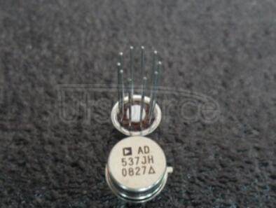
AD537JH The AD537 is a monolithic V-F converter consisting of an input amplifier, a precision oscillator system, an accurate internal reference generator and a high current output stage. Only a single external RC network is required to set up any full-scale (F.S.) frequency up to 100 kHz and any F.S. input voltage up to ±30 V. Linearity error is as low as ±0.05% for 10 kHz F.S., and operation is guaranteed over an 80 dB dynamic range. The overall temperature coefficient (excluding the effects of external components) is typically ±30 ppm/°C. The AD537 operates from a single supply of 5 V to 36 V and consumes only 1.2 mA quiescent current.
A temperature-proportional output, scaled to 1.00 mV/K, enables the circuit to be used as a reliable temperature-to-frequency converter<br/> in combination with the fixed reference output of 1.00 V, offset scales such as 0°C or 0°F can be generated.
The low drift (1μV/°C typ) input amplifier allows operation directly from small signals (e.g., thermocouples or strain gages) while offering a high (250 M(Ohm) input resistance. Unlike most V-F converters, the AD537 provides a square-wave output, and can drive up to 12 TTL loads, LEDs, very long cables, etc.
The excellent temperature characteristics and long-term stability of the AD537 are guaranteed by the primary bandgap reference generator and the low T.C. silicon chromium thin film resistors used throughout.
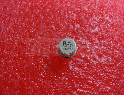
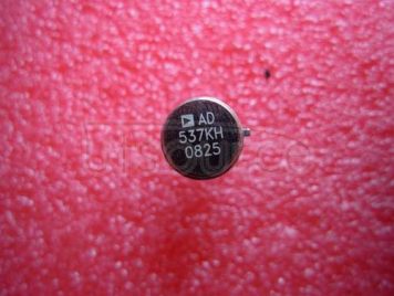
The device is available in either a TO-116 ceramic DIP or a TO-100 metal can<br/> both are hermetically sealed packages.
The AD537 is available in three performance/temperature grades<br/> the J and K grades are specified for operation over the 0°C to +70°C range while the AD537S is specified for operation over the extended temperature range, -55°C to +125°C.
  • AD537JH
  • AD537JH
販売数量 :3
113521

5.0 つ星のうち5

1 star 0.3%
2 star 0%
3 star 0.2%
4 star 0.4%
5 star 99.1%

商品合計:2398055

合計:12724315

Average lead time: 0 時間

配達時間(速達): 0

配達時間(郵便局): 0

お気に入り

AD537JH

USED

Utsource certified used parts

Utsource認定済みの中古部品は、次の保証を提供します。

1. Utsourceは、外観検査(外観に深刻な損傷がない)を含む商品を検査し、資格のある正直なサプライヤーを選択し、98%の資格率を保証します。

2.一部の部品は機械でテストされています。

3. Utsource認定部品は、60日以内であれば無条件で返品および返金できます。

製品の説明

The AD537 is a monolithic V-F converter consisting of an input amplifier, a precision oscillator system, an accurate internal reference generator and a high current output stage. Only a single external RC network is required to set up any full-scale (F.S.) frequency up to 100 kHz and any F.S. input voltage up to ±30 V. Linearity error is as low as ±0.05% for 10 kHz F.S., and operation is guaranteed over an 80 dB dynamic range. The overall temperature coefficient (excluding the effects of external components) is typically ±30 ppm/°C. The AD537 operates from a single supply of 5 V to 36 V and consumes only 1.2 mA quiescent current. A temperature-proportional output, scaled to 1.00 mV/K, enables the circuit to be used as a reliable temperature-to-frequency converter
in combination with the fixed reference output of 1.00 V, offset scales such as 0°C or 0°F can be generated. The low drift (1μV/°C typ) input amplifier allows operation directly from small signals (e.g., thermocouples or strain gages) while offering a high (250 M(Ohm) input resistance. Unlike most V-F converters, the AD537 provides a square-wave output, and can drive up to 12 TTL loads, LEDs, very long cables, etc. The excellent temperature characteristics and long-term stability of the AD537 are guaranteed by the primary bandgap reference generator and the low T.C. silicon chromium thin film resistors used throughout. The device is available in either a TO-116 ceramic DIP or a TO-100 metal can
both are hermetically sealed packages. The AD537 is available in three performance/temperature grades
the J and K grades are specified for operation over the 0°C to +70°C range while the AD537S is specified for operation over the extended temperature range, -55°C to +125°C.

見つかりません、同様のデータシートをお勧めします

  • ECAD Module
  • Series: -
  • Brand: Analog Devices
  • DateCode: 96+
  • Package / Case: CAN-10
  • Packaging: Bulk
  • Part Status: Active
  • Type: Voltage to Frequency
  • Frequency - Max: 100kHz
  • Full Scale: ±30ppm/°C
  • Linearity: ±0.05%
  • Mounting Type: Through Hole
  • Supplier Device Package: TO-100-10
類似モデル VFC32

このサイトで使用されているすべての製品名、商標、ブランド、ロゴは、それぞれの所有者の財産です。 これらの名前、商標、ブランド、およびロゴを使用した製品の描写、説明、または販売は、識別のみを目的としており、権利所有者との提携または許可を示すことを意図したものではありません。

ECAD Module

製品の属性

  • AD537JH is a monolithic integrated circuit from Analog Devices. It is a precision, low-cost, low-power, single-supply, 8-bit analog-to-digital converter (ADC). Description: The AD537JH is an 8-bit, low-power, low-cost, single-supply, monolithic ADC. It operates from a single +5 V supply and features a fast conversion rate of 10 μs. The AD537JH has an input range of 0 V to +5 V and a reference input range of 0 V to +5 V. It features an on-chip reference and a built-in reference buffer. Features: 8-bit resolution Low power consumption Single +5 V supply Fast conversion rate of 10 μs Input range of 0 V to +5 V Reference input range of 0 V to +5 V On-chip reference Built-in reference buffer Applications: The AD537JH is suitable for a wide range of applications including data acquisition systems, instrumentation systems, and industrial process control systems. It is also suitable for use in medical imaging systems, automotive systems, and consumer electronics. (For reference only)

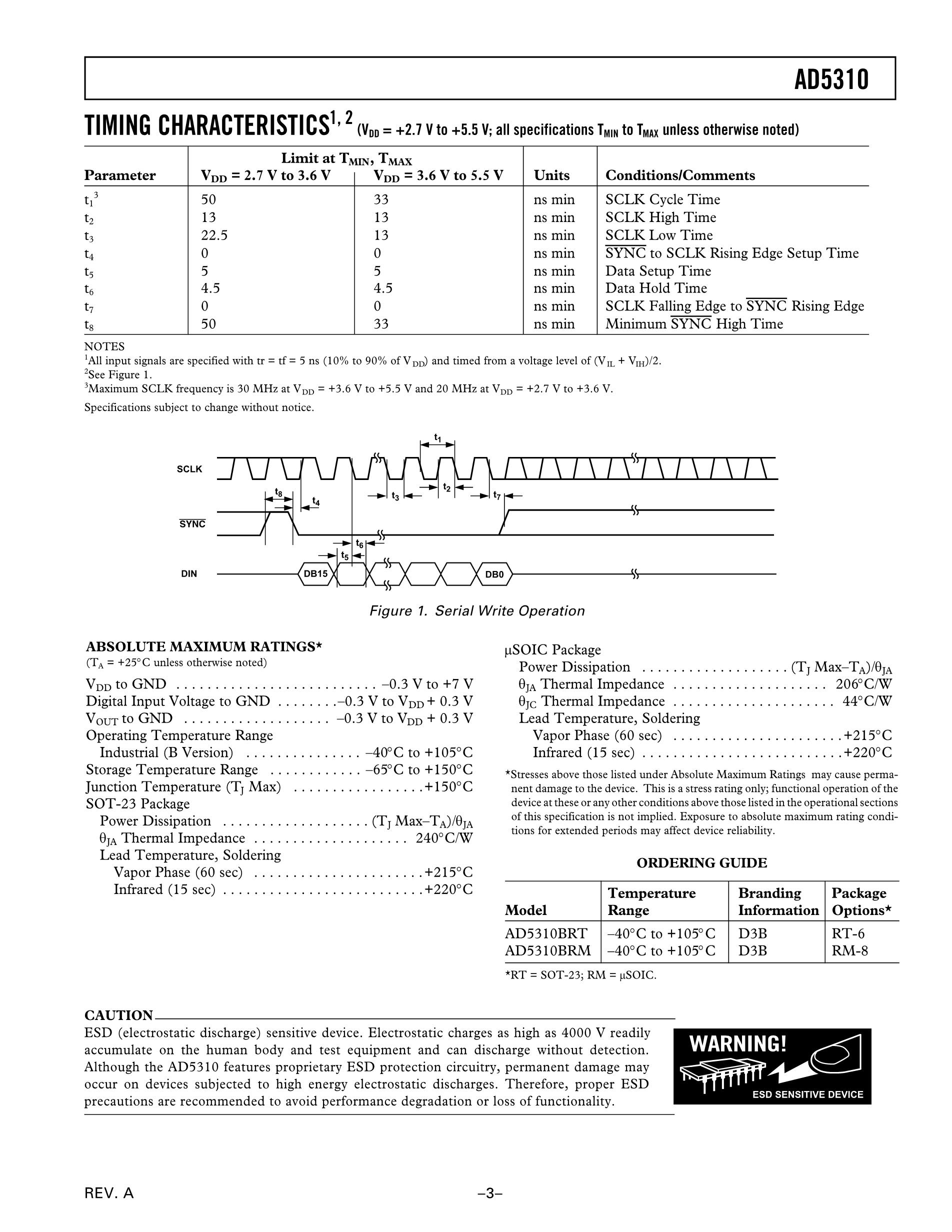
データシートの最初の 3 ページのプレビュー

  • AD537JH's pdf picture 1
  • AD537JH's pdf picture 2
  • AD537JH's pdf picture 3

ドキュメントのプレビュー

AD537­SPECIFICATIONS (typical @ +25C with VS (total) 36 V, unless otherwise noted)

fMAX = 10 kHz fMAX = 100 kHz Full-Scale Calibration Error = 0.01 µF, IIN 1.000 mA vs. Supply (fMAX < 100 kHz) vs. Temp (TMIN to TMAX)

Single Supply Dual Supply Input Bias Current
0 to (+VS ­ 4) Volts (min) ­VS to (+VS ­ 4) Volts (min)
(Trimmable in "D" Package Only) vs. Supply vs. Temp (TMIN to TMAX) Safe Input Voltage3
vs. Temp (TMIN to TMAX) vs. Supply Output Resistance4 Absolute Temperature Reference5
Initial Calibration @ +25°C Slope Error from 1.00 mV/K
VOUT 0.4 V max (TMIN to TMAX) 20 mA min Output Leakage Current in Logic "1"
(TMIN to TMAX) Logic Common Level Range

**Specifications same 1Nonlinearity is specified for a current input level (IIN) to the converter from to 1000 µA. Converter has 100% overrange capability up to IIN 2000 µA with slightly reduced linearity. Nonlinearity is defined as deviation from a straight line from zero to full scale, expressed as a percentage of full scale. 2Guaranteed not tested. 3Maximum voltage input level is equal to the supply on either input terminal. However, large negative voltage levels can be applied to the negative terminal if the input is scaled to

a nominal 1 mA full scale through an appropriate value resistor (See Figure 2). 4Loading the 1.0 volt or 1 mV/K outputs can cause a significant change in overall circuit performance, as indicated in the applications section. To maintain normal operation,

these outputs should be operated into the external buffer or an external amplifier. 5Temperature reference output performance is specified from to +70°C for "J" and "K" devices, to +125°C for "S" model. 6D = Ceramic DIP; H = Hermetic Metal Can. For outline information see Package Information section. 7For AD537/883B specifications, refer to Analog Devices Military Products Databook.

CIRCUIT OPERATION Block diagrams of the AD537 are shown above. A versatile operational amplifier (BUF) serves as the input stage; its purpose is to convert and scale the input voltage signal to a drive current in the NPN follower. Optimum performance is achieved when, at the full-scale input voltage, 1 mA drive current is delivered to the current-to-frequency converter. The drive current to the current-to-frequency converter (an astable multivibrator) provides both the bias levels and the charging current to the externally connected timing capacitor. This "adaptive" bias scheme allows the oscillator to provide low nonlinearity over the entire current input range to 2000 µA. The square wave oscillator output goes to the output driver which provides a floating base drive to the NPN power transistor. This floating drive allows the logic interface to be referenced to a different level than ­VS. The "SYNC" input ("D" package only) allows the oscillator to be slaved to an external master oscillator; this input can also be used to shut off the oscillator.

The reference generator uses a bandgap circuit (this allows single-supply operation to 4.5 volts which is not possible with low T.C. Zeners) to provide the reference and bias levels for the amplifier and oscillator stages. The reference generator also provides the precision, low T.C. 1.00 volt output and the VTEMP output which tracks absolute temperature at 1 mV/K.

V-F CONNECTION FOR POSITIVE INPUT VOLTAGES The positive voltage input range is from ­VS (ground in single supply operation) to 4 volts below the positive supply. The connection shown in Figure 1 provides a very high (250 M) input impedance. The input voltage is converted to the proper drive current at Pin 3 by selecting a scaling resistor. The full-scale current is 1 mA, so, for example a 10 volt range would require a nominal 10 k resistor. The trim range required will depend on capacitor tolerance. Full-scale currents other than 1 mA can be chosen, but linearity will be reduced; mA is the maximum allowable drive.

As indicated by the scaling relationship in Figure 0.01 µF timing capacitor will give a 10 kHz full-scale frequency, and 0.001 µF will give 100 kHz with 1 mA drive current. The maximum frequency is 150 kHz. Polystyrene or NPO ceramic capacitors are preferred for T.C. and dielectric absorption; polycarbonate or mica are acceptable; other types will degrade linearity. The capacitor should be wired very close to the AD537.

Figure 1. Standard V-F Connection for Positive Input Voltages

V-F CONNECTIONS FOR NEGATIVE INPUT VOLTAGE OR CURRENT A wide range of negative input voltages can be accommodated with proper selection of the scaling resistor, as indicated in Figure 2. This connection, unlike the buffered positive connection, is not high impedance since the 1 mA F.S. drive current must be supplied by the signal source. However, very large negative voltages beyond the supply can be handled easily; just modify the scaling resistors appropriately. Diode (HP50822811) is necessary for overload and latchup protection for current or voltage inputs.

If the input signal is a true current source, R1 and R2 are not used. Full-scale calibration can be accomplished by connecting 200 k pot in series with a fixed 27 k from Pin 7 to ­VS (see calibration section, below).

Figure 2. V-F Connections for Negative Input Voltage or Current

CALIBRATION There are two independent adjustments: scale and offset. The first is trimmed by adjustment of the scaling resistor R and the second by the (optional) potentiometer connected to +VS and the VOS pins ("D" package only). Precise calibration requires the use of an accurate voltage standard set to the desired FS value and a frequency meter; a scope is useful for monitoring output waveshape. Verification of linearity requires the availability of a switchable voltage source (or a DAC) having a linearity error below ± 0.005%, and the use of long measurement intervals to minimize count uncertainties. Every AD537 is automatically tested for linearity, and it will not usually be necessary to perform this verification, which is both tedious and time-consuming.

Although drifts are small it is good practice to allow the operating environment to attain stable temperature and to ensure that the supply, source and load conditions are proper. Begin by setting the input voltage 1/10,000 of full scale. Adjust the offset pot until the output frequency 1/10,000 of full scale (for example 1 Hz for of 10 kHz). This is most easily accomplished using a frequency meter connected to the output. Then apply the FS input voltage and adjust the gain pot until the desired FS frequency is indicated. In applications where the FS input is small, this adjustment will very slightly affect the offset voltage, due to the input bias current of the buffer amplifier. A change in R will affect the input by approximately 100 µV, which is as much mV FS range. Therefore, it may be necessary to repeat the offset and scale adjustments for the highest accuracy. The design of the input amplifier is such that the input voltage drift after offset nulling is typically below l µV/°C.

同じデータシートの関連製品

ADG812
. Bandwidth -3 dB (typ) : 90MHz, Isupply Pos (max) : 1µA, Supply Voltage Type: single/dual/multi : Single,
AD8315
. # of Channels : 1, Min Positive Supply Voltage : 2.7V, Max Positive Supply Voltage : 5.5V, Supply Voltage
ADL5513S
. # of Channels : 1, Min Positive Supply Voltage : 2.7V, Max Positive Supply Voltage : 5.5V, Supply Voltage
AD7690
. VSupply Unipolar : Yes, ADC Output Sample Rate (max) : 400kSPS, Vref Source : External, Signal to Noise
AD7175-2
. VSupply Unipolar : No, ADC Output Sample Rate (max) : 250kSPS, Vref Source : External, Internal, Signal
AD7730
. VSupply Unipolar : Yes, ADC Output Sample Rate (max) : 1.2kSPS, Vref Source : External, Signal to Noise
ADAS3022
. VSupply Unipolar : No, ADC Output Sample Rate (max) : 1MSPS, Vref Source : External, Internal, Signal
LTC2153-14
. ADC Output Sample Rate (max) : 310MSPS, Vref Source : External, Internal, Signal to Noise + Distortion
AD9910
. # of Channels : 1, Vref Source : Internal, Min Positive Supply Voltage : 1.8V, Max Positive Supply Voltage
ADP2370
. Synchronous : Yes, Monolithic : Yes, Vout Min : 800mV, Output Current : 800mA, Number of Outputs : 1, Integrated

同じメーカーの部品番号

同じカテゴリ

ADVFC32KN
IC CONV V/F F/V 0-70DEGC 14-DIP
AD537JD
IC V/F CONV 14-CDIP
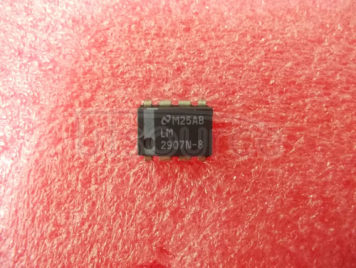
LM2907N-8
LM2907/LM2917 Frequency to Voltage Converter
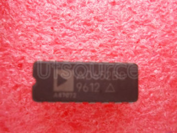
AD652BQ
Monolithic Synchronous Voltage-to-Frequency Converter
VFC32KP
Voltage-to-Frequency and Frequency-to-Voltage Converter 14-PDIP
AD537KH
Integrated Circuit Voltage-to-Frequency Converter
AD652AQ
Monolithic Synchronous Voltage-to-Frequency Converter
ADVFC32KN
IC VFC32 V/F-F/V CONVERTER
商品レビュー

    Submit

    Japan からの 44 件のバイヤーレビュー

    Alternate Text

    hirabayashi makoto

    SI8642BC-B-IS1
    jp Japan gyoda-city

    Length of registration:2 years

    good!

    0

    0

    もとに戻す0

    10/07/2021

    Alternate Text

    Tsuyoshi Shimizu

    T2563
    jp Japan Komatsu, Fuefuki city

    Length of registration:2 years

    satisfaction

    0

    0

    もとに戻す0

    07/29/2021

    Alternate Text

    Mitsunaga Saito

    TC74HC4040AP
    jp Japan TUKUBASHI

    Length of registration:6 years

    OK.best friend

    0

    0

    もとに戻す0

    09/15/2020

    Alternate Text

    Satoshi Shibuichi

    27C256-10
    jp Japan Kamakura-City

    Length of registration:3 years

    Works fine!

    0

    0

    もとに戻す0

    05/17/2020

    Alternate Text

    tsutsui kenzi

    M57762
    jp Japan Kawagoe city

    Length of registration:7 years

    Thank you.

    0

    0

    もとに戻す0

    05/05/2020

    Alternate Text

    Ito Kenji

    TA7179M
    jp Japan hannan

    Length of registration:8 years

    Very satisfied with

    0

    0

    もとに戻す0

    05/03/2020

    Alternate Text

    Shoichi Wakaguri

    Disposable Masks, Mask (500 pcs) (U.S.A. region only)
    jp Japan Tokyo

    Length of registration:7 years

    Very Good Quality MASKS!

    0

    0

    もとに戻す0

    04/18/2020

    Alternate Text

    goro miyake

    2SB1243TV2Q
    jp Japan takamatsu, kagawa-pref.

    Length of registration:9 years

    OK.

    0

    0

    もとに戻す0

    12/14/2017

    Alternate Text

    Kazumori Tanaka

    GS-R405S
    jp Japan GAMAGORI

    Length of registration:11 years

    They are very good goods. Thank you!!

    0

    0

    もとに戻す0

    10/21/2016

    Alternate Text

    Mitsuru Kawamoto

    3SK228
    jp Japan Sapporo City

    Length of registration:7 years

    good job thanks!

    0

    0

    もとに戻す0

    07/01/2016

    Alternate Text
    See all reviews >>

    支払い方法

    欧州決済方法

    Alternate Text

    アジア決済方法

    Alternate Text

    アメリカア決済方法

    Alternate Text

    国際決済方法

    Alternate Text

    ショッピングの流れ

    • ウェブサイトで検索
      お問い合わせを送信
    • 買い物カゴに追加
      照会カートに追加
      お見積り
    • 注文
    • 商品の倉庫保管
      包装
      発送注文
    ショッピングガイド 関連検索 関連サプライ 別名
    ショッピングガイド

    注文

    • ユーザーは、部品をカートに追加して部品を検索するときにBOMをアップロードし、1秒でコストを計算し、最高の部品表を提供できます。
    • 一部の特定の製品は、最小注文数量に到達する必要があります。
    • plusメンバーを適用すると、ユーザーはランダムにクーポンを取得できます。 Utsourceは、注文時にさまざまな販売店からさまざまな製品品質のさまざまな購入オプションを提供しています。
    • ユーザーは「お問い合わせカート」に製品を追加してお問い合わせを送信できます。utsourceから見積メールが送信されます。
    • 税金の請求書や備考などの追加の注文手順を追加する必要がある場合は、注文情報ページに記載してください。
    • すべての注文情報は「アカウントセンター」ページで確認できます
    • ご注文の際は商品説明をご確認ください。
    • 発送後に注文をキャンセルすることはできないため、発送前にカスタマーサービスにメールで注文の詳細を修正してください。
    • UtsourceモバイルブラウザのバージョンとAPPをダウンロードして、必要に応じていつでもどこでもパーツを見つけることができます。
    • 必要に応じて、注文する言語と通貨を選択してください。

    支払い

    • UTSOURCEは、主流を含むグローバルな支払いをサポートしています US PAYPAL、クレジットカード(VISA、MASTERCARD、AMERICAN EXPRESS、JCB)、WEST UNION、Moneygram;
    • ヨーロッパで人気のある支払い:SofortBanking、Trustpay、Paysafecard;
    • 中東:CashU、Onecard;
    • 東南アジア:MOLPay;
    • ロシアが一般的に使用するもの:Qiwi、Yandex Money、WebMoney;
    • オランダの支払い:iDEAL、ポーランド語Dotpay、
    • ブラジルの支払い:Boleto
    • これらの上記の支払いは、ローカルエリアで高い市場シェアを有しており、より良い支払い経験、より簡単な支払い方法を備えています。

    送料

    • USPS、FedEx、DHL、およびUPSを選択できます。
    • エクスプレス:(FEDEX、UPS、DHL、TNT)200ドル以上のご注文で最初の0.5kgが送料無料、重量超過は別途請求されます。
    • ユーザーは、要件に応じて「Freight Collect」を選択できます
    • 遠隔地にいる場合は、配送に追加の遠隔料金がかかる場合があります。
    • ご注文の送料は、ショッピングカートで自動的に計算されます。送料についてご不明な点がございましたら、お気軽にお問い合わせください。手動で確認させていただきます。
    • 在庫のあるパーツの場合、注文は通常1〜2日で発送されます。
    • 納期:通常2〜5営業日。
    • 配送追跡番号はメールで送信されます。または、注文が発送されたら、APPまたはWebサイトの「アカウントセンター」にアクセスして確認できます。
    • 請求書は、必要に応じて「アカウントセンター」>「私の請求書」からダウンロードできます

    ギフトクーポン/プラスサービス

    • 5米ドルの配送クーポンを受け取ることができます(新規ユーザーに適用)
    • 30日間のPLUS無料試用サービスを提供します(試用期間の終了後、plusサービスは自動的に停止され、追加料金は発生しません。商品価格は通常10%引き下げられます)
    • 「Fundsアカウント」は、「Fundsアカウント」に返金されたお金がある場合、次の注文の購入に使用できます。 ([マイアカウント]> [ファンドアカウント]で確認できます)
    • Utsourceは、米国、メキシコ、ブラジル、イタリア、フランス、ドイツ、およびその他の多くの場所で、世界中でプロフェッショナルなカスタマーサービスを提供しています。

    戻る

    返品は通常、荷物の配達日から60日以内に完了すると受け付けられます。

    欠陥(不適合製品の第三者品質報告書を提供してください)

    返送料金は前払いする必要があります。 代金引換貨物は受け付けません。

    保証ポリシー

    すべてのUTSOURCEの購入には、60日間の返金返品ポリシーに加えて、製造上の欠陥に対する90日間のUTSOURCE保証があります。この保証は、不適切な顧客の組み立て、顧客による指示に従わないこと、製品の変更によって欠陥が生じたアイテムには適用されません。 、過失または不適切な操作。

    関連検索
    • AD537JH 価格
    • AD537JH Pdf
    • AD537JH 見つけにくい
    • AD537JH ピン配列
    • AD537JH 時代遅れ
    • AD537JH イメージ
    • AD537JH 購入
    • AD537JH 画像
    • AD537JH 売る
    • AD537JH 在庫あり
    • AD537JH 検索
    • AD537JH ディストリビューター
    • AD537JH データシート
    • AD537JH 正規品
    • AD537JH 応用
    • AD537JH シリーズ
    • AD537JH 置換
    • AD537JH TI(Analog Devices)
    • AD537JH find
    • AD537JH purchase
    • AD537JH need
    • AD537JH shopping
    • AD537JH store
    • AD537JH 安いです
    • AD537JH transistor
    • AD537JH equivalent
    • AD537JH 電子部品
    • AD537JH The AD537 is a monolithic V-F converter consisting of an input amplifier, a precision oscillator system, an accurate internal reference generator and a high current output stage. Only a single external RC network is required to set up any full-scale (F.S.) frequency up to 100 kHz and any F.S. input voltage up to ±30 V. Linearity error is as low as ±0.05% for 10 kHz F.S., and operation is guaranteed over an 80 dB dynamic range. The overall temperature coefficient (excluding the effects of external components) is typically ±30 ppm/°C. The AD537 operates from a single supply of 5 V to 36 V and consumes only 1.2 mA quiescent current. A temperature-proportional output, scaled to 1.00 mV/K, enables the circuit to be used as a reliable temperature-to-frequency converter
      in combination with the fixed reference output of 1.00 V, offset scales such as 0°C or 0°F can be generated. The low drift (1μV/°C typ) input amplifier allows operation directly from small signals (e.g., thermocouples or strain gages) while offering a high (250 M(Ohm) input resistance. Unlike most V-F converters, the AD537 provides a square-wave output, and can drive up to 12 TTL loads, LEDs, very long cables, etc. The excellent temperature characteristics and long-term stability of the AD537 are guaranteed by the primary bandgap reference generator and the low T.C. silicon chromium thin film resistors used throughout. The device is available in either a TO-116 ceramic DIP or a TO-100 metal can
      both are hermetically sealed packages. The AD537 is available in three performance/temperature grades
      the J and K grades are specified for operation over the 0°C to +70°C range while the AD537S is specified for operation over the extended temperature range, -55°C to +125°C.
    関連サプライ
    モデル 販売元名称 在庫 ブランド カプセル化 ロット番号 製品の説明 価格
      別名

      AD537JH

      AD537JHには世界中にいくつかのブランドがあり、地域の違いや買収によりAD537JHの別名が付けられる場合があります。 AD537JHは次の名前でも知られています。

        Alternate Text

        購入オプション

        在庫状態: 5000

        最小数量: 1

        買い物カゴに追加

        合計額:

        単価:5211

        • ≥1: ¥5211.00000 ¥4690.00000
        • ≥2: ¥5211.00000 ¥4690.00000
        • ≥5: ¥5037.00000 ¥4534.00000
        • ≥10: ¥4968.00000 ¥4471.00000
        • ≥20: ¥4933.00000 ¥4440.00000
        • ≥30: ¥4864.00000 ¥4377.00000
        • ≥50: ¥4864.00000 ¥4377.00000
        • ≥100: ¥4829.00000 ¥4346.00000
        • ≥500: ¥4794.00000 ¥4315.00000
        もっと: 引き合い 価格比較

        UTSOURCE 公式

        国:

        United States

        • Afghanistan
        • Albania
        • Algeria
        • American Samoa
        • Andorra
        • Angola
        • Anguilla
        • Antarctica
        • Antigua and Barbuda
        • Argentina
        • Armenia
        • Aruba
        • Australia
        • Austria
        • Azerbaijan
        • Bahamas
        • Bahrain
        • Bangladesh
        • Barbados
        • Belarus
        • Belgium
        • Belize
        • Benin
        • Bermuda
        • Bhutan
        • Bolivia
        • Bosnia and Herzegovina
        • Botswana
        • Bouvet Island
        • Brazil
        • British Indian Ocean Territory
        • Brunei Darussalam
        • Bulgaria
        • Burkina Faso
        • Burundi
        • Cambodia
        • Cameroon
        • Canada
        • Cape Verde Islands
        • Cayman Islands
        • Central African Republic
        • Chad
        • Chile
        • China
        • Christmas Island
        • Cocos (Keeling) Islands
        • Colombia
        • Comoros
        • Congo (DEM. REP. OF)
        • Congo (REP. OF)
        • Cook Islands
        • Costa Rica
        • Cote D'Ivoire
        • Croatia
        • Cuba
        • Curacao
        • Cyprus
        • Czech Republic
        • Denmark
        • Djibouti
        • Dominica
        • Dominican Republic
        • Ecuador
        • Egypt
        • El Salvador
        • Equatorial Guinea
        • Eritrea
        • Estonia
        • Ethiopia
        • Falkland Islands (Malvinas)
        • Faroe Islands
        • Federated States of Micronesia
        • Fiji
        • Finland
        • France
        • French Guiana
        • French Polynesia
        • French Southern Territories
        • Gabon
        • Gambia
        • Georgia
        • Germany
        • Ghana
        • Gibraltar
        • Greece
        • Greenland
        • Grenada
        • Guadeloupe
        • Guam
        • Guatemala
        • Guinea
        • Guinea-bissau
        • Guyana
        • Haiti
        • Heard and Mc Donald Islands
        • Honduras
        • Hong Kong
        • Hungary
        • Iceland
        • India
        • Indonesia
        • Iran (Islamic Republic of)
        • Iraq
        • Ireland
        • Israel
        • Italy
        • Jamaica
        • Japan
        • Jordan
        • Kazakhstan
        • Kenya
        • Kiribati
        • Kosovo
        • Kuwait
        • Kyrgyzstan
        • Lao People's Democratic Republic
        • Latvia
        • Lebanon
        • Lesotho
        • Liberia
        • Libyan Arab Jamahiriya
        • Liechtenstein
        • Lithuania
        • Luxembourg
        • Macau
        • Macedonia
        • Madagascar
        • Malawi
        • Malaysia
        • Maldives
        • Mali
        • Malta
        • Marshall Islands
        • Martinique
        • Mauritania
        • Mauritius
        • Mayotte
        • Mexico
        • Micronesia
        • Moldova
        • Monaco
        • Mongolia
        • Montenegro
        • Montserrat
        • Morocco
        • Mozambique
        • Myanmar
        • Namibia
        • Nauru
        • Nepal
        • Netherlands
        • Netherlands Antilles
        • New Caledonia
        • New Zealand
        • Nicaragua
        • Niger
        • Nigeria
        • Niue
        • Norfolk Island
        • North Korea
        • Northern Mariana Islands
        • Norway
        • Oman
        • Pakistan
        • Palau
        • Panama
        • Papua New Guinea
        • Paraguay
        • Peru
        • Philippines
        • Pitcairn
        • Poland
        • Portugal
        • Puerto Rico
        • Qatar
        • Reunion
        • Romania
        • Russia
        • Rwanda
        • Saint Kitts and Nevis
        • Saint Lucia
        • Saint Vincent and the Grenadines
        • Samoa
        • San Marino
        • Sao Tome and Principe
        • Saudi Arabia
        • Senegal
        • Serbia
        • Serbia and Montenegro
        • Seychelles
        • Sierra Leone
        • Singapore
        • Slovakia (Slovak Republic)
        • Slovenia
        • Solomon Islands
        • Somalia
        • South Africa
        • South Georgia & South Sandwich Islands
        • South Korea
        • Spain
        • Sri Lanka
        • St. Helena
        • St. Pierre and Miquelon
        • Sudan
        • Suriname
        • Svalbard and Jan Mayen Islands
        • Swaziland
        • Sweden
        • Switzerland
        • Syrian Arab Republic
        • Tahiti
        • Taiwan
        • Tajikistan
        • Tanzania
        • Thailand
        • Togo
        • Tokelau
        • Tonga
        • Trinidad and Tobago
        • Tunisia
        • Turkey
        • Turkmenistan
        • Turks and Caicos Islands
        • Tuvalu
        • Uganda
        • Ukraine
        • United Arab Emirates
        • United Kingdom
        • United States
        • United States minor outlying islands
        • Uruguay
        • Uzbekistan
        • Vanuatu
        • Vatican City State (Holy See)
        • Venezuela
        • Vietnam
        • Virgin Islands (British)
        • Virgin Islands (U.S.)
        • Wallis and Futuna Islands
        • Western Sahara
        • Yemen
        • Zambia
        • Zimbabwe
        • キャリア 送料 輸送時間
        • 0.00 3-5 days
        • 0.00 3-5 days
        • 0.00 3-5 days
        • 7.99 8-12 days
        • Alternate Text
          0.00 5-8 days
        • Alternate Text
          0.00 6-10 days
        • Alternate Text
          0.00 6-10 days
        • Alternate Text
          0.00 8-10 days
        • Alternate Text
          0.00 15-20 days
        • Alternate Text
          0.00 15-18 days
        • Alternate Text
          0.00 8-10 days
        • Alternate Text
          0.00 7-10 days
        • Alternate Text
          0.00 10-12 days
        • Alternate Text
          0.00 3-5 days
        • Alternate Text
          0.00 2-3 days

        速達:(FEDEX, UPS, DHL, TNT)¥28405以上のご注文で、最初の0.5kg配送料無料。超過分は別途請求。

        Alternate Text

        Judy顧客管理者

        sales@utsource.com

        (888) 766 5577

        +86 15302769052

        +1 (312)899-4831

        (whatsapp only)

        いつでも最高のサービスを提供する、専用のカスタマーサービス。

        videoImg
        videoImg
        videoImg
        videoImg
        videoImg
        Alternate Text

        通貨:

        Alternate Text Alternate Text Alternate Text

        製品 中古

        生産の専門家を停止し、生産を停止し、見つけるのが難しい多数の電子部品を提供し、メンテナンス会社を促進することができます

        Alternate Text 在庫

        在庫なし

        在庫なし

        Reply to

        submit
        ×
        AF AL DZ AS AD AO AI AQ AG AR AM AW AU AT AZ BS BH BD BB BY BE BZ BJ BM BT BO BA BW BV BR IO BN BG BF BI KH CM CA CV KY CF TD CL CN CX CC CO KM CD CG CK CR CI HR CU AN CY CZ DK DJ DM DO EC EG SV GQ ER EE ET FK FO FM FJ FI FR GF PF TF GA GM GE DE GH GI GR GL GD GP GU GT GN GW GY HT HM HN HK HU IS IN ID IR IQ IE IL IT JM JP JO KZ KE KI YK KW KG LA LV LB LS LR LY LI LT LU MO MK MG MW MY MV ML MT MH MQ MR MU YT MX FM MD MC MN ME MS MA MZ MM NA NR NP NL AN NC NZ NI NE NG NU NF KP MP NO OM PK PW PA PG PY PE PH PN PL PT PR QA RE RO RU RW KN LC VC WS SM ST SA SN RS CS SC SL SG SK SI SB SO ZA GS KR ES LK SH PM SD SR SJ SZ SE CH SY PF TW TJ TZ TH TG TK TO TT TN TR TM TC TV UG UA AE GB US UM UY UZ VU VA VE VN VG VI WF EH YE ZM ZW

        フリーダイヤル

        (888) 766 5577 USA & カナダ

        +52 5515436027
        +52 5515436028 メキシコ

        +49 6931090199 ドイツ

        +55 21 3609 8727 ブラジル

        (800) 137235 イタリア

        (900) 649657 スペイン

        Whatsapp

        +1 (312) 899-4831 USA

        +49 15217848563 ドイツ

        +52 55 7637 4368 メキシコ

        E-mail

        sales@utsource.com

        国際支払

        グローバルロジスティクス

        footShip
        Copyright © 2022 Power by UTSOURCE INTERNATIONAL LIMITED ISO/IEC 20000-1:2011,ISO/IEC 27001:2013 鄂ICP备2021003526号-1